QTREX produces cryogenic chip carrier using single-build AME process
QTREX Quantum (Nasdaq: QTEX) has produced a cryogenic chip carrier using its proprietary single-build additively manufactured electronics (AME) process, the company said on 18 June 2026. The carrier was made to a design supplied by an unnamed US-based technology company described as one of the world's largest developers of full-stack quantum computing systems.
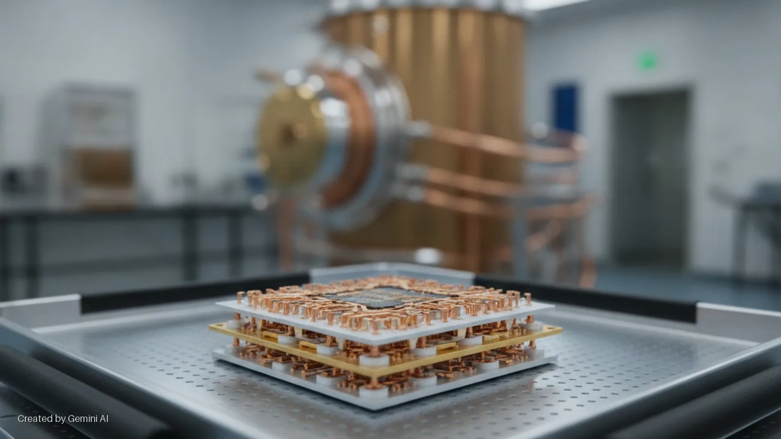
The announcement marks a strategic expansion for the Nes Ziona-based firm, which has until now focused primarily on cryogenic signal transport and interconnects. A chip carrier sits at the processor-interface layer of the quantum hardware stack, physically supporting the quantum processor and managing signal fan-out between the processor and the cryogenic I/O stack beneath it.
What the technology does
QTREX's carrier uses a Kapton-class polyimide architecture adapted for operation at very low temperatures, typical of dilution cryostat environments. The single-build AME process integrates conductive pathways, dielectric structures, electromagnetic shielding features and direct interconnect transitions into a single monolithic component, rather than assembling them from separate parts with conventional connectors.
The company says the approach is intended to reduce potential failure points, lower thermal load and support higher routing density than connector-based alternatives. Because shielding is engineered directly into the structure and AME enables three-dimensional routing geometries, QTREX argues the design can address the signal-integrity and channel-count demands that arise as quantum processors scale to larger qubit numbers.
Chief executive Dagi Ben-Noon said the milestone "represents a meaningful expansion of our position within the quantum hardware ecosystem" and that the capability "further strengthens QTREX's role in addressing one of the fundamental scaling challenges facing the quantum computing industry." The company did not disclose yield data, thermal performance figures, or the identity of the partner company.
The next phase, QTREX said, will involve designing customer-specific carriers tailored to individual processor architectures. The company plans to present the physical sample during private meetings in Boston around the Quantum.Tech World 2026 conference on 25 to 26 June.
Market context
Cryogenic packaging and interconnect is an increasingly crowded niche as quantum hardware companies move from laboratory demonstrations toward engineered systems capable of hosting hundreds or thousands of physical qubits. Conventional PCB and connector-based architectures face limits in routing density, thermal load and reliability at millikelvin temperatures, creating commercial openings for specialist component vendors.
QTREX competes in this space against established defence and aerospace electronics manufacturers as well as a small number of startups targeting the quantum packaging layer specifically. The unnamed US customer is likely among the handful of well-resourced full-stack quantum programmes, including those operated by IBM, Google, Microsoft and Amazon, though QTREX did not confirm this.
The broader quantum hardware supply chain remains at an early stage of commercialisation. Most revenue in the sector still flows from government research contracts, cloud-access partnerships and consortium grants rather than volume component sales. For QTREX, which also carries a medical technology portfolio it is seeking to monetise separately, the chip carrier milestone is a proof of manufacturing capability rather than a confirmed commercial win. Investors will be looking for a named customer, a supply agreement, and performance benchmarks before treating this as a material revenue event.