Nokia expands Pennsylvania photonic chip facility tenfold for AI
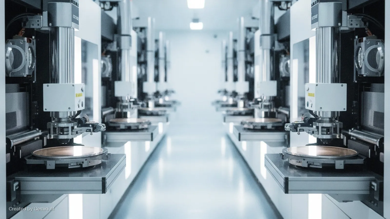
Nokia has announced a significant expansion of its advanced test and packaging (ATP) facility in Allentown, Pennsylvania, targeting up to a tenfold increase in production capacity for photonic chips used in optical networking modules. The company says new capacity will be commercially available by the end of the third quarter of 2026, and the investment is expected to nearly double the site's workforce to more than 500 roles spanning engineering, manufacturing, and research and development.
The Allentown expansion carries a total investment of approximately $30 million, which includes roughly $10 million in federal CHIPS and Science Act investment tax credits and around $4 million in assistance from the Commonwealth of Pennsylvania. The move forms part of Nokia's broader, multi-year commitment to invest $4 billion in US-based research, development, and manufacturing oriented around AI-ready network connectivity.
The deal
Nokia's Allentown facility is one of only a handful of US sites carrying out ATP of photonic chips into optical modules. The company points out that less than two percent of global semiconductor ATP currently takes place in the United States, positioning the Allentown site as a strategically significant node in domestic supply chains for critical communications infrastructure.
Justin Hotard, President and Chief Executive of Nokia, said the expansion reflects "the strong partnership between Nokia, the United States, and the Commonwealth of Pennsylvania to support advanced manufacturing, create jobs, and strengthen US technology leadership and global competitiveness." The company also claims its optical networking technologies can reduce energy usage in AI communications by as much as 75 percent compared with conventional alternatives, though it did not publish a supporting third-party benchmark in the release.
A projected economic impact of more than $500 million over five years was cited in the announcement, alongside endorsements from Pennsylvania Governor Josh Shapiro, Senator Dave McCormick, Congressman Ryan Mackenzie, and Bill Frauenhofer, Executive Director of Semiconductor Investment and Innovation at the Department of Commerce.
Market context
The announcement arrives at a moment of heightened policy focus on domestic semiconductor supply chains. The CHIPS and Science Act, signed in 2022, has catalysed a wave of manufacturing commitments from both US and international vendors seeking to diversify production away from East Asian concentration. ATP in particular has historically been concentrated in Taiwan, South Korea, and Malaysia, and Washington has identified packaging capacity as a critical gap in the US semiconductor ecosystem.
Nokia's photonic chip work sits at the intersection of two high-priority spending categories: AI infrastructure buildout and optical networking for next-generation telecom. Hyperscalers are investing heavily in custom silicon and high-bandwidth optical interconnects as GPU cluster densities grow, creating demand for exactly the kind of low-latency, energy-efficient optical modules Nokia produces in Allentown. Competitors in the optical networking space include Coherent, Lumentum, and II-VI, as well as vertically integrated hyperscaler programmes developing in-house photonic components.
The energy efficiency claim is commercially significant. AI data centres face mounting pressure over power consumption from grid operators, regulators, and sustainability-focused investors. A 75 percent reduction in energy use for AI communications, if substantiated at scale, would be a notable differentiator in procurement decisions, particularly in jurisdictions with constrained grid capacity or carbon commitments.
Regulatory read-across
The federal CHIPS investment tax credit applied here is distinct from the direct fabrication grants awarded to leading-edge logic fabs. Nokia's eligibility underlines that the programme's scope extends to advanced packaging, an area the US Department of Commerce has explicitly prioritised in its national semiconductor strategy. Companies drawing on CHIPS incentives are subject to guardrails on expansion in countries of concern, including restrictions on material capacity increases in China for a ten-year period. Nokia has not indicated that those constraints affect its existing operations.
The next milestones to watch are the commercial availability confirmation at the end of Q3 2026, publication of independent energy-efficiency benchmarks, and any customer announcements that tie Allentown output to named AI infrastructure deployments.