
Applied Materials launches seven systems for AI chip DRAM and packaging
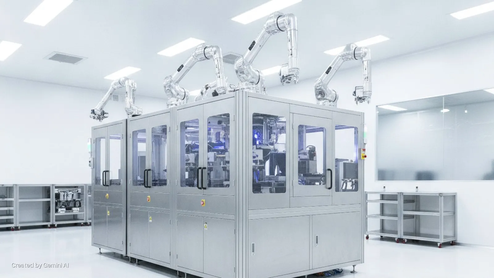
Applied Materials (Nasdaq: AMAT) has introduced a suite of seven new semiconductor manufacturing systems designed to address two of the most pressing bottlenecks in AI chip production: DRAM performance scaling and the precision demands of advanced 3D packaging. The announcements were timed to coincide with the company's DRAM and Advanced Packaging Master Class held on 25 June 2026.
The headline product is an enhanced version of the Centura Prime Epi epitaxy system, updated to selectively grow doped silicon germanium and silicon phosphorous in transistor source and drain regions. Applied says the technique, long established in leading-edge logic, is now becoming critical in DRAM peripheral transistors as memory makers chase the bandwidth requirements of high bandwidth memory (HBM) and next-generation DDR. The revised system also carries a 20% smaller footprint than its predecessor, allowing denser tool deployment within existing fab layouts.
Advanced packaging: three new process tools
The bulk of the announcement addresses advanced packaging, an area Applied describes as now strategically equivalent to on-chip transistor scaling. Three new process systems target specific yield challenges in HBM and chiplet-based designs.
The Opta Quad CMP platform handles chemical mechanical planarisation for advanced packaging, where thicker films and tighter tolerances increase the risk of surface non-uniformity. It monitors wafer conditions in real time and adjusts polish parameters dynamically, a capability Applied positions as critical for hybrid bonding, where two chip surfaces must achieve near-perfect planarity before copper-to-copper fusion.
The Nokota VMax 2 electrochemical deposition system fills through-silicon vias (TSVs) and forms microbumps for 3D stacking. It introduces a feature Applied calls Adaptive Pattern Tuning, which shapes the electric field during copper plating to compensate for layout-driven variation across the wafer.
The Producer Avila 2 PECVD system deposits stress-balanced dielectric films around TSVs in ultra-thin DRAM dies, which are thinned to roughly 1/25th the thickness of a standard wafer for HBM stacking. Applied says the system supports reliable stacking of 12-layer and 16-layer HBM designs, with future higher layer counts in scope.
Metrology extended to packaging
Applied also announced two eBeam systems ported from its wafer-fab portfolio to advanced packaging environments. The VeritySEM 7AP provides critical dimension metrology with sub-10 nm sensitivity on thick, warped and heterogeneous substrates common in HBM and chiplet architectures. The SEMVision G7AP extends Applied's defect analysis platform to silicon, organic and glass packaging substrates. Applied says the SEMVision G7AP is already running in production at undisclosed memory and logic manufacturers.
Prabu Raja, President of the Semiconductor Products Group at Applied Materials, said: "The transistor and materials technologies that drove performance gains in leading-edge logic are now becoming essential in DRAM. As DRAM scales to meet the bandwidth demands of HBM and AI workloads, the distinction between logic and memory process technology is converging."
Market context
Applied Materials competes in semiconductor process equipment against ASML, Lam Research, KLA Corporation and Tokyo Electron, with each vendor holding strong positions in specific process steps. The advanced packaging segment has grown substantially as chipmakers including TSMC, Samsung and SK Hynix invest heavily in HBM capacity to meet demand from AI accelerator customers such as Nvidia. Analyst estimates have consistently placed HBM as one of the fastest-growing segments in the broader memory market through the late 2020s.
The broader competitive dynamic in packaging equipment is shifting. TSMC's CoWoS and SoIC platforms, along with Samsung's X-Cube architecture, are placing increasingly exacting requirements on CMP uniformity and TSV fill quality, creating a direct commercial opportunity for the tools Applied has now formalised. Export control considerations remain a background factor: US BIS restrictions on advanced semiconductor equipment exports to certain jurisdictions continue to shape where Applied's customers can deploy capacity, and further tightening of those controls could affect order flows for advanced packaging tools specifically.