Applied Materials unveils ALD and etch systems for 3D chip scaling
Applied Materials has introduced two new semiconductor processing systems designed to address one of the more pressing manufacturing challenges at advanced nodes: maintaining precise materials control inside the tall, narrow structures that define modern 3D chip architectures. The systems, announced on 15 June 2026 alongside the IEEE VLSI Symposium, target both logic and memory chipmakers working at the leading edge of AI compute hardware.
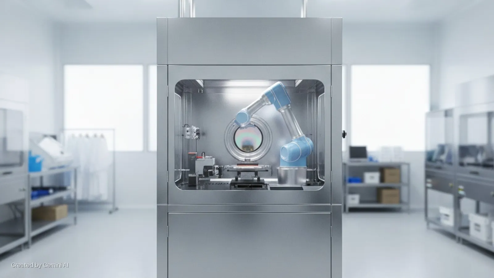
The two products are the Centris Spectral SiN ALD and the Producer Selectra Mo Etch. According to the company, both are already in use at unnamed leading logic and memory fabs, with the Mo Etch system described as validated in high-volume manufacturing.
What the systems do
The Centris Spectral SiN ALD addresses a well-known limitation of conventional plasma-enhanced deposition: as 3D structures grow taller and narrower, traditional plasma sources struggle to distribute process chemistry uniformly from the top of a feature to its base. Applied says its system solves this using a high-density microwave plasma that achieves dense, uniform silicon nitride films at low temperatures, even in challenging high-aspect-ratio geometries. Silicon nitride is widely used for surface passivation, dielectric isolation and patterning spacers, and its quality directly affects transistor performance and yield. In gate-all-around transistors specifically, the company says the system can form contact liners that reduce resistance and capacitance at critical interfaces.
The system sits within Applied's broader Spectral ALD platform, a quad-reactor tool family with configurable plasma and thermal processing and support for both temporal and spatial atomic layer deposition modes.
The Producer Selectra Mo Etch targets a different scaling bottleneck in 3D NAND. As layer counts increase, molybdenum is being adopted for wordline metallisation because of its low resistance, but isolating individual wordlines in deep stacks has become difficult for legacy wet etch processes. Liquid chemistries lose uniformity with depth, producing top-heavy etch profiles that degrade yield and data retention. Applied says its dry etch system delivers superior top-to-bottom uniformity and tighter profile control, reducing cell-to-cell variability and lowering leakage. The Selectra portfolio previously covered dielectric and silicon applications; Mo Etch extends it into metal integration, with the company noting potential applications across NAND, DRAM and foundry logic.
Prabu Raja, President of the Semiconductor Products Group at Applied Materials, said: "From transistor structures to memory stacks, chipmakers need new ways to precisely deposit and selectively remove materials in extremely complex 3D architectures."
Market and competitive context
Applied Materials competes in semiconductor process equipment against ASML, Lam Research, Tokyo Electron and KLA. Deposition and etch are two of the highest-value process steps in terms of tool count per wafer, and both categories have seen intensifying competition as chipmakers migrate from planar to 3D device geometries. Lam Research has been an incumbent in high-aspect-ratio etch, particularly for 3D NAND; Applied's move into selective metal etch for molybdenum wordlines is a direct push into territory Lam has traditionally occupied.
The timing is significant. TSMC is ramping gate-all-around production for its N2 node, Samsung is advancing its 3nm GAA process, and major NAND producers including Samsung, SK Hynix and Micron are competing on layer count. Each transition creates fresh equipment qualification cycles, and a system already validated in high-volume manufacturing carries a credible advantage in those cycles.
From a regulatory standpoint, both systems are aimed squarely at the leading-edge nodes subject to US export controls administered by the Bureau of Industry and Security. Equipment of this type requires export licences for sales to certain jurisdictions, a constraint that has become a recurring commercial consideration for all US-headquartered semiconductor equipment companies. Applied did not address export-control implications in its release.
The new tools will be highlighted at the 2026 IEEE VLSI Technology and Circuits Symposium, where Applied is also hosting a panel on co-optimising system architecture, logic, memory and packaging for AI-driven compute workloads.