Riber accelerates ROSIE oxide-epitaxy platform toward commercial scale
Riber, the Bezons-based molecular beam epitaxy (MBE) equipment manufacturer listed on Euronext Growth Paris, used its Annual General Meeting on 17 June 2026 to detail progress on ROSIE, its oxide-on-silicon epitaxy platform, and to reaffirm a commercialisation roadmap it says is on track despite longer sales cycles in its core MBE business.
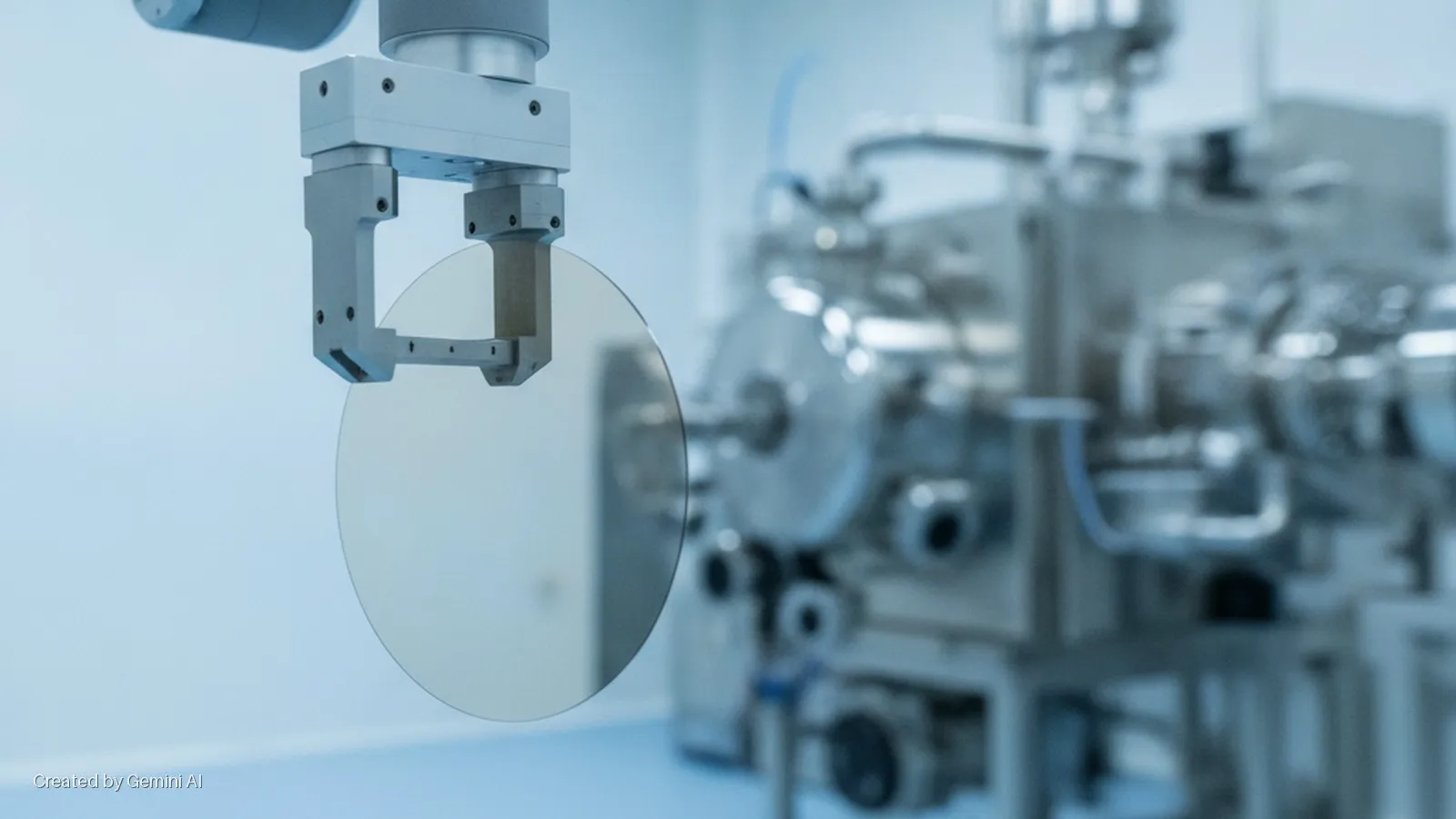
The company said initial titanium dioxide and strontium peroxide depositions on 300 mm silicon wafers had demonstrated thickness non-uniformity of just 1%, meeting the process specification required before the more strategically significant barium titanate and strontium titanate layers can be grown. Those BTO/STO samples, to be made available to scientific and industrial partners through Riber's collaboration with the Novo Nordisk Foundation Quantum Computing Programme, represent the platform's first credible commercial proof points.
ROSIE: milestones and near-term deliverables
Beyond the deposition results, Riber disclosed that it expects to deliver a second ROSIE system "shortly" to an unnamed leading quantum computing company in the United States. The company did not identify the customer, the contract value, or a precise delivery date. It also said it plans to complete a dual-chamber cluster ROSIE production system by the end of 2026, positioned to handle an anticipated ramp in customer demand once BTO/STO sample availability triggers evaluation cycles.
Chairwoman Annie Geoffroy framed the platform's significance in the context of rising capital flows into AI infrastructure and quantum technology. "In an environment characterised by accelerating global investments in artificial intelligence, data infrastructure and quantum technologies, RIBER is executing its roadmap with determination," she said, adding that the ROSIE programme "strengthens our confidence in our ability to support the transformation of the semiconductor industry."
The company also acknowledged that its existing MBE equipment business is experiencing extended customer decision cycles, attributed to the increasing complexity of customer projects and tighter export-licence requirements for shipments to China. That regulatory friction, driven by US Bureau of Industry and Security controls on advanced semiconductor equipment and broadly mirrored by European export policy, is a headwind for any manufacturer whose MBE systems touch compound semiconductor and quantum research programmes in controlled jurisdictions.
Market context and competitive landscape
Functional oxide deposition on 300 mm silicon wafers sits at the intersection of two fast-moving markets: silicon photonics for data-centre interconnects and quantum-device fabrication. The data-centre photonics opportunity is supported by surging AI-driven bandwidth demand, with hyperscalers and co-location operators deploying co-packaged optics and electro-optic modulators at scale. Riber is positioning ROSIE as an enabling deposition platform for the electro-optic components those architectures require.
The competitive landscape for oxide epitaxy on silicon is still forming. Established thin-film deposition vendors such as Applied Materials and Tokyo Electron address the broader silicon process equipment market but have not, to date, publicly targeted functional-oxide-on-silicon at the 300 mm wafer standard with a dedicated platform. Riber's MBE heritage gives it process depth in complex heterostructure growth, though converting that into volume semiconductor equipment revenue requires qualification cycles that typically run 18 to 36 months at advanced-node fabs.
The planned dual-chamber cluster system is an important step toward fab-compatible throughput, but volume production credibility will depend on named customer wins, published yield data and, ultimately, integration into a qualified pilot line. The NQCP partnership is intended to provide exactly that qualification pathway, targeting photonic and quantum technology pilot-line integration. Investors and prospective customers will be watching for BTO/STO sample results and the identity of the US quantum-computing customer as the primary near-term signals of commercial momentum.