
Soitec and ZenSemi partner to scale 300mm BCD-on-SOI production
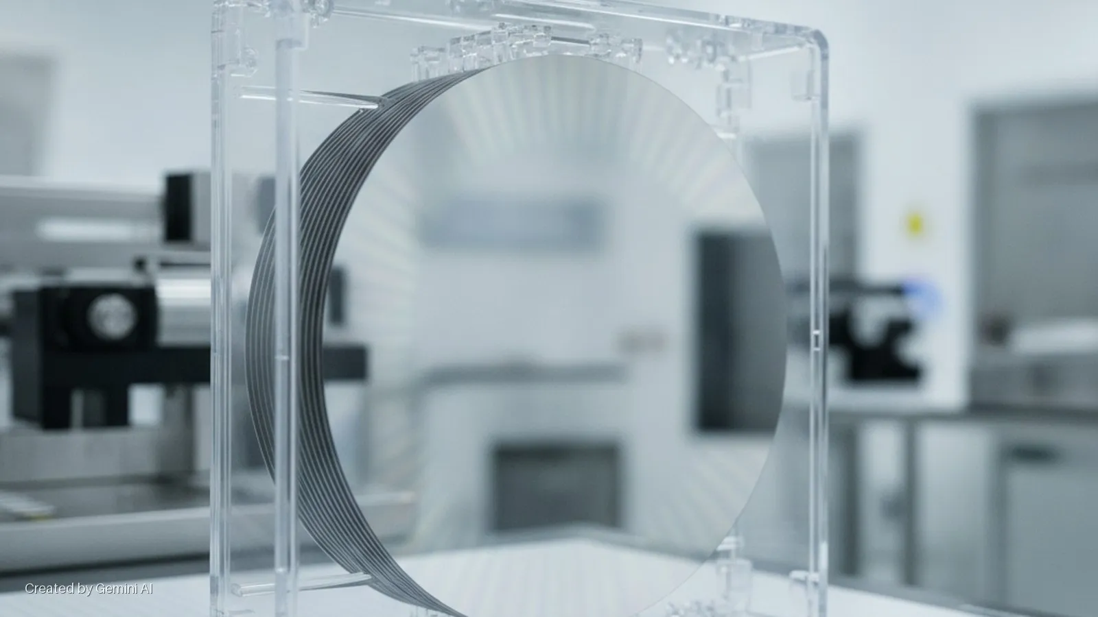
Soitec and ZenSemi have announced a strategic collaboration to bring high-volume 300mm BCD-on-SOI (Bipolar-CMOS-DMOS on Silicon-on-Insulator) technology to market, targeting power electronics used in AI data centres, electric vehicles, humanoid robots and industrial automation. Under the arrangement, Soitec will supply its engineered 300mm Power-SOI substrates to ZenSemi's specialty foundry in Guangzhou, supporting both process development and a capacity ramp-up that the two companies say will serve fabless designers and integrated device manufacturers globally.
ZenSemi's vice president of sales and marketing, Ruby Yan, said that first-silicon validation with the firm's lead customer has already demonstrated a roughly 30% die size reduction for an 18-channel analogue front-end device compared with traditional bulk BCD processes. That figure, if reproducible at volume, is a meaningful differentiator in markets where board space and thermal density are hard constraints.
Why BCD-on-SOI matters
BCD-on-SOI uses full dielectric isolation to eliminate parasitic latch-up and reduce electrical crosstalk, allowing high-voltage power stages and sensitive low-voltage control circuitry to coexist on a single chip. The approach is not new, but moving it to 300mm wafers is significant: the larger format drives down per-die cost and makes the technology accessible to a broader range of customers who previously faced a capacity shortage or had to accept higher costs from 200mm fabs.
René Jonker, chief product officer at Soitec, framed the deal as evidence that the BCD-on-SOI supply chain in China is maturing. Soitec, which reported revenue of 600 million euros in its 2025-26 fiscal year and holds close to 4,800 patents, has long positioned engineered substrates as a route to both performance gains and energy efficiency, and the power electronics segment is now one of its three core strategic markets alongside mobile communications and edge AI.
Market and competitive context
The partnership lands at a time when power-management IC demand is under pressure from several directions simultaneously. AI data centre buildouts are driving demand for efficient high-voltage power delivery. Automotive electrification is pulling in chips that must meet ISO 26262 functional safety (FuSa) standards. And the humanoid-robotics segment, while still early-stage, is beginning to attract serious semiconductor investment.
Competing foundry platforms for BCD-on-SOI work exist at established players in Europe and the United States, but 300mm capacity specifically for this process node is limited. ZenSemi's existing fab, which the company describes as the first 300mm facility built exclusively for MEMS and CMOS, gives it an unusual substrate from which to add BCD-on-SOI capacity, though the ramp timeline and volume commitments have not been disclosed.
The collaboration also carries a geopolitical dimension worth noting. Soitec is a French-listed company supplying advanced substrate technology to a Chinese foundry at a moment when semiconductor supply-chain sovereignty is a live policy concern in both Brussels and Washington. While Power-SOI substrates are not currently subject to the most stringent US Bureau of Industry and Security export-control classifications applied to leading-edge logic, any tightening of controls on speciality semiconductor materials could affect the commercial terms of this arrangement. Buyers relying on ZenSemi capacity will want to monitor that policy environment closely.
Next milestones
Neither company disclosed a timeline for full-volume production, specific capacity targets, or pricing for the Power-SOI substrate supply agreement. The parties said they intend to make the platform available to both domestic Chinese design houses and international customers, with automotive, AI infrastructure and industrial automation cited as the primary end markets. Progress on customer qualification and functional safety certifications will be the key indicators to watch as the partnership moves from first-silicon validation to production ramp.