
Wooptix installs first Phemet metrology system at CEA-Leti
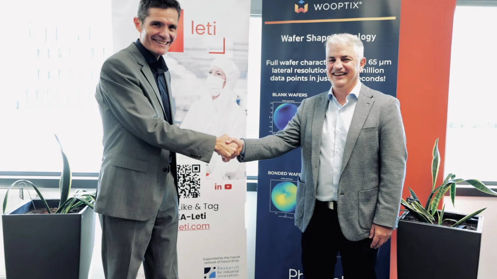
Wooptix has completed the first installation of its Phemet wafer-shape and geometry metrology system at CEA-Leti's technology research institute in Grenoble, marking the inaugural production deployment of the platform. The system was installed on 4 May 2026, and the partnership was formally highlighted at CEA-Leti Innovation Days in late June.
The collaboration will centre on joint work covering wafer-scale process signatures, nanotopography, and advanced packaging metrology, all conducted inside an industrial semiconductor cleanroom operating at 300 mm wafer scale. Wooptix introduced Phemet in November 2025, describing it as a fully automated platform capable of sub-nanometre resolution measurement of wafer shape and geometry using wavefront phase imaging (WFPI), a technique derived from adaptive optics research in astronomy.
The collaboration
José Manuel Ramos, chief executive of Wooptix, said the CEA-Leti installation represents "a necessary step in our roadmap toward high-volume semiconductor manufacturing applications" and will allow the company to build application evidence around real process-development challenges. He noted that the Grenoble presence strengthens Wooptix's foothold in what he described as a dynamic European semiconductor hub.
Viorel Balan, collaboration project manager at CEA-Leti, said the institute intends to use the Phemet platform to deepen understanding of nanotopographic processes, support EU research programmes, and accelerate development of next-generation advanced packaging technologies. CEA-Leti brings significant infrastructure to the partnership: the institute operates more than 14,000 square metres of cleanroom space, holds a portfolio of 3,200 patents, and employs a staff of over 2,000 researchers. It has launched 80 startups since its founding in 1967.
Neither party disclosed the financial terms of the joint agreement, the duration of the collaboration, or any committed commercialisation milestones.
Market context
Semiconductor metrology is under increasing pressure as chipmakers push toward sub-2nm nodes and heterogeneous integration through advanced packaging techniques such as chiplets and 3D stacking. Tighter process control at each manufacturing step is essential when feature sizes and layer-to-layer alignment tolerances shrink to the nanoscale. The metrology and process-control segment is dominated by established players including KLA Corporation and Onto Innovation, while a number of smaller, venture-backed specialists are seeking to differentiate on specific measurement modalities such as optical, electron-beam, and now wavefront-based techniques.
Wooptix's WFPI approach is positioned by the company as offering speed and resolution advantages for in-line, non-destructive wafer inspection, a capability that is becoming commercially significant as advanced packaging volumes grow alongside demand for AI accelerator silicon. A placement at CEA-Leti, one of Europe's most widely referenced pre-industrialisation facilities, carries credibility value: tier-one chipmakers and equipment suppliers regularly use CEA-Leti as a neutral proving ground before committing to volume procurement.
Regulatory and policy read-across
The collaboration is also relevant in the context of European semiconductor policy. The EU Chips Act, which entered force in 2023, targets a doubling of Europe's share of global chip production to 20 percent by 2030 and includes provisions for strengthening the research and pilot-line ecosystem. CEA-Leti is a named participant in several EU-funded research programmes, and Balan explicitly noted that Phemet work will support EU project commitments. For Wooptix, a Spain-headquartered startup with offices in Tenerife, Madrid, and Grenoble, embedding the technology in EU-funded research pipelines could materially accelerate commercial adoption by European fabs and integrated device manufacturers.
The next milestones investors and customers will look for are published benchmark data from the CEA-Leti deployment, named commercial customers beyond the research context, and any indication of when Wooptix intends to pursue volume production agreements.