
Navitas wins U.S. Army ALATTIS contract for 10 kV SiC semiconductors
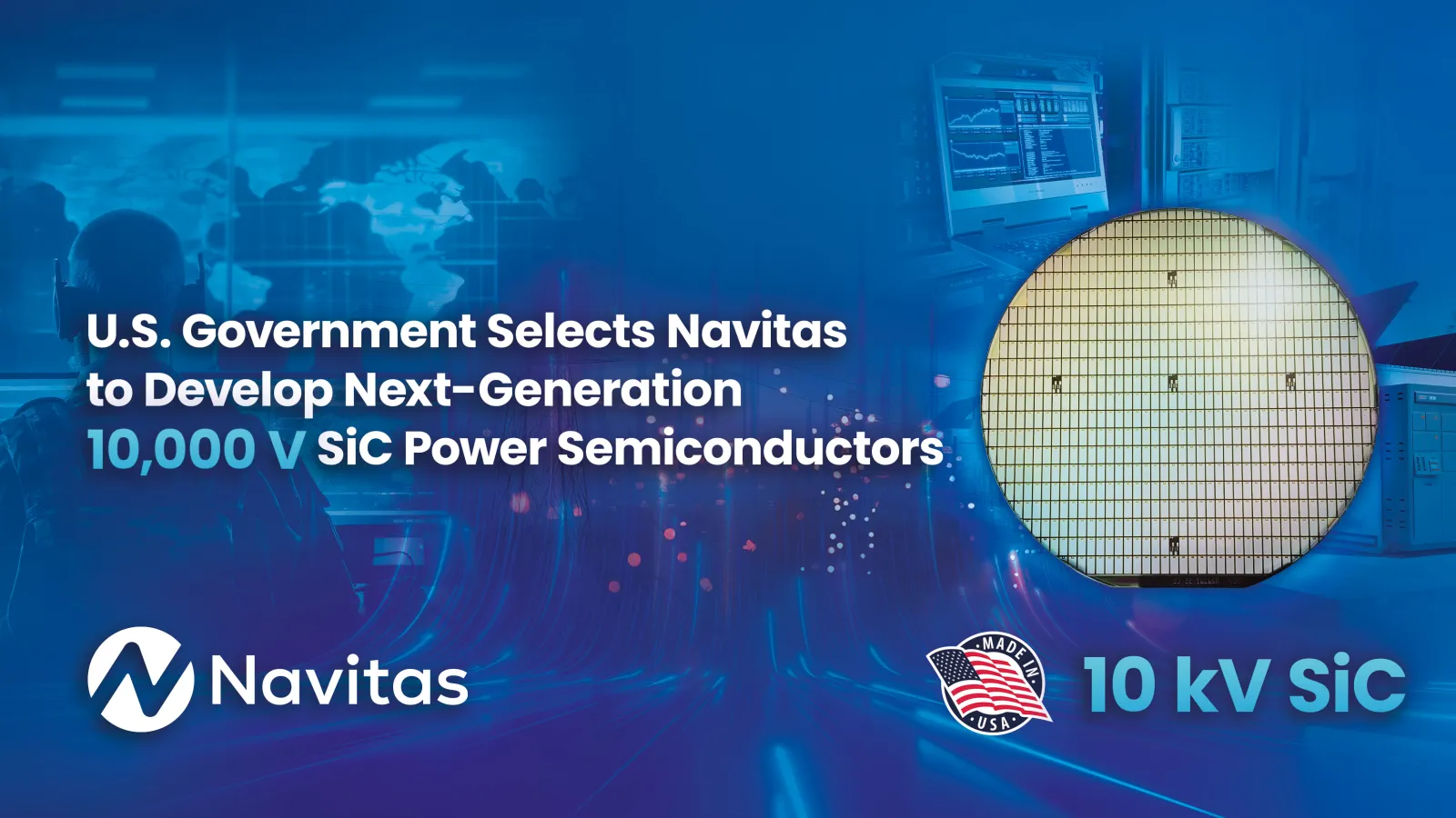
Navitas Semiconductor (Nasdaq: NVTS) has been selected by the U.S. Army to lead the ALATTIS (Accelerated, Large-Area, 10 kV SiC IGBT) programme, a government-funded prototype project to develop and validate a domestic manufacturing process for ultra-high-voltage silicon carbide (SiC) power semiconductor devices. The award follows a competitive evaluation and was made by the Army Research Laboratory (ARL), operating under DEVCOM, with backing from the Joint Experimentation and Technology Accelerator (JETX).
The programme targets 10 kV insulated-gate bipolar transistors (IGBTs) and associated PiN diode technologies for mission-critical Armed Forces systems. Navitas said it will build on its patented trench-assisted planar (TAP) MOSFET architecture, which currently spans voltage ratings from 650 V to 6.5 kV across its GeneSiC portfolio. The ALATTIS work represents an extension beyond that existing range.
The award
Siddarth Sundaresan, SVP and Chief Technology Officer at Navitas, said the contract "enables Navitas to extend its leadership beyond SiC MOSFETs by developing next-generation 10 kV SiC IGBTs built on our unique, patented trench-assisted planar (TAP) architecture and integrated with advanced PiN diode technologies." The company cited a track record spanning more than two decades in ultra-high-voltage SiC, including 6.5 kV SiC thyristors recognised with an R&D 100 Award in 2010, 10-15 kV PiN diodes in 2012, and commercial release of 6.5 kV SiC MOSFETs in 2021.
Navitas did not disclose the contract value, programme duration, or specific performance milestones. The release describes the project as a prototype programme, indicating it remains in a pre-production phase, with commercialisation timelines not yet stated.
Market context and competitive positioning
The push to domestic ultra-high-voltage SiC manufacturing sits at the intersection of two significant policy trends: U.S. efforts to onshore critical semiconductor supply chains, accelerated by the CHIPS and Science Act, and defence procurement requirements for secure, domestically produced components. Power semiconductors rated at 10 kV and above are relevant to grid infrastructure, electric vehicle fast-charging at scale, and high-power military platforms such as directed-energy systems and next-generation radar.
The wide-bandgap semiconductor space is increasingly competitive. Wolfspeed remains the largest dedicated SiC manufacturer by capacity, while onsemi, STMicroelectronics, and Infineon have each invested heavily in SiC wafer and device production. Navitas occupies a differentiated position through its combined GaN and SiC portfolio, but it is a considerably smaller company by revenue than these incumbents. A government prototype contract, while not a volume production award, provides engineering credibility and can serve as a pathway to follow-on procurement.
Regulatory and supply-chain read-across
The ALATTIS programme's emphasis on a "U.S.-anchored" manufacturing ecosystem reflects broader federal concern about dependence on overseas suppliers for advanced power devices. U.S. export controls administered by the Bureau of Industry and Security (BIS) already restrict certain semiconductor manufacturing equipment, and the Defence Department has been tightening requirements around trusted foundry status for components used in weapons systems. A validated domestic 10 kV SiC process would address a gap that currently has no commercially available U.S. source, according to the programme's own framing.
Navitas holds more than 300 issued or pending patents and describes itself as the first semiconductor company to achieve CarbonNeutral certification. The company also serves commercial markets including AI data centres and grid infrastructure, meaning the underlying TAP architecture developed under ALATTIS could have dual-use commercial applications, though any such roadmap was not discussed in the release.