
ASM launches PECVD flowable carbon film for 3D chip scaling
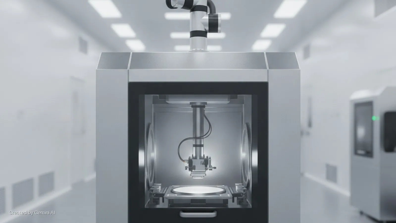
ASM International has launched the XP8 Vertos Flowable Carbon, which the Dutch semiconductor equipment maker describes as the first plasma-enhanced chemical vapour deposition (PECVD) flowable carbon film to combine gap fill and planarisation in a single process step. The product is now in initial high-volume manufacturing deployment and is applicable across both logic and memory device architectures.
The launch addresses a structural problem that has accumulated over two decades of semiconductor scaling. Conventional carbon films deposit material conformally, meaning any surface irregularity from one process step propagates into the next, requiring additional fill, etch-back or chemical mechanical planarisation (CMP) to correct. As device architectures push into complex three-dimensional structures with high-aspect-ratio features, that multi-step remediation becomes increasingly costly in time, yield and defect risk.
How Vertos works
Tyler Sample, Vice President and PECVD Key Product Unit Head at ASM, explained the core distinction: where incumbent carbon films conform to feature shapes and inherit their topography problems, the Vertos material flows into features from the bottom up, filling without voids or seams before self-planarising across the wafer surface. The result, the company says, is a flat, uniform substrate ready for the next patterning step without downstream CMP or etch-back. The process runs on an all-in-one PECVD platform, which ASM says reduces both cost-per-wafer and sources of defect introduction.
Unique film properties cited by ASM include improved planarisation across substrates with varied pattern density, higher thermal stability than existing carbon films, and area selective deposition characteristics. The thermal stability point is commercially significant: patterning processes in advanced nodes must survive elevated temperatures elsewhere in the integration stack without film degradation, a constraint that has historically limited the usability of flowable dielectric approaches in carbon applications.
Chief executive Hichem M'Saad said that every chip built with the technology "represents faster, more efficient AI performance for the people and industries that depend on it," framing the launch squarely within the AI-driven compute demand that has reshaped semiconductor equipment spending over the past two years.
Market context
ASM occupies a focused niche within the semiconductor equipment landscape, competing primarily in atomic layer deposition and epitaxy against larger rivals including Applied Materials, Lam Research and Tokyo Electron. Patterning-related materials and deposition steps have become a high-value battleground as EUV lithography alone cannot resolve the complexity of the most advanced 3D NAND and gate-all-around logic node integration schemes. The ability to reduce process step count is commercially attractive to chipmakers managing escalating cost-per-layer as vertical NAND stacks grow beyond 300 layers and logic nodes shrink below 2nm.
The Semiconductor Industry Association projected the global semiconductor market would reach $1.5 trillion in revenue during 2026, a figure ASM cited in its release. That broader market context has concentrated equipment spending on the materials and deposition categories where ASM competes, providing a favourable environment for the Vertos launch.
ASM did not disclose customer names, volume commitments, or pricing for the XP8 Vertos platform. The company also did not state which foundry or integrated device manufacturer is the initial high-volume manufacturing partner. Investors and process engineers will look for named customer wins and published yield data as the primary validation milestones in the quarters ahead. The technology's scalability claim across current and future nodes will require demonstration across at least two process generations before it can be assessed independently of ASM's own characterisation.