
Intel Foundry ships first high-volume logic product on ASML High NA EUV
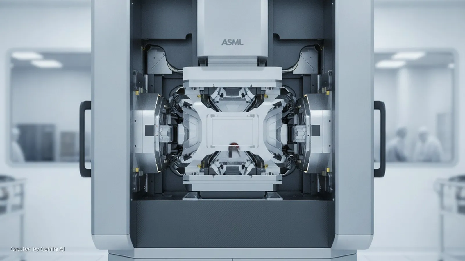
Intel Foundry has begun shipping a subset of its Intel Core Ultra Series 3 processors, code-named Panther Lake, manufactured using ASML's High NA EUV (extreme ultraviolet) lithography equipment on the Intel 18A process node. The announcement, made jointly by ASML and Intel on 15 July 2026, marks the first time any chipmaker has shipped a high-volume logic product patterned with High NA EUV, extending a collaboration between the two companies that stretches back decades.
Specific layers within the Intel 18A process have been dual-qualified on the High NA EUV platform at Intel's Hillsboro, Oregon, site, with yields reported to match those achieved on the existing NXE (standard NA) EUV toolset. Intel Foundry executive vice president Naga Chandrasekaran said qualifying the High NA EUV process option on select product layers allows the existing tool fleet to deliver increased output for customers, while the partnership develops further options for upcoming nodes.
What the milestone means
High NA EUV uses a higher numerical aperture optical system than the previous generation of EUV scanners, enabling finer patterning resolution and tighter overlay accuracy. ASML's production-generation tool, the TWINSCAN EXE:5200B, was first installed and acceptance-tested at Intel's Hillsboro R&D site, following the integration of the original TWINSCAN EXE:5000 in 2024. The improved light source and overlay performance of the 5200B are designed to support continued transistor density scaling at the angstrom-era nodes that follow Intel 18A.
ASML president and chief executive Christophe Fouquet described the development as "a substantial development in semiconductor lithography," noting that smaller, denser patterning would accelerate progress in AI and other compute-intensive applications. Intel and ASML did not disclose throughput figures, per-wafer cost data, or the volume share of Panther Lake units manufactured using High NA EUV versus the standard NXE platform.
Market context and competitive read-across
The introduction of High NA EUV into production is consequential for the broader semiconductor industry. TSMC and Samsung, the other two leading-edge fabs, have both received TWINSCAN EXE systems for evaluation, but neither has publicly confirmed high-volume production use. Intel Foundry's claim to be first in the industry to ship HVM logic on High NA EUV represents a meaningful datapoint in its effort to rebuild credibility as an external foundry, following years of process delays that ceded ground to TSMC.
Intel 18A is the node on which Intel Foundry is pitching prospective fabless customers. Demonstrating that a commercially shipping product has been successfully patterned using the next-generation litho platform strengthens that pitch, even where High NA EUV is initially used on a limited subset of layers. Analysts have noted that full layer coverage with High NA EUV is expected at subsequent nodes rather than at 18A, where the tool is principally being used to build manufacturing confidence and accumulate process data.
Regulatory and supply considerations
ASML's EXE-series systems are subject to Dutch and EU export-control restrictions that currently prevent shipment to certain jurisdictions, most notably China. The High NA EUV ramp is therefore initially confined to fabs in the United States, Europe and Taiwan, a constraint that has geopolitical as well as commercial implications for chipmakers assessing long-term node roadmaps. The US CHIPS and Science Act, which provides incentive funding for Intel's Oregon and Ohio fab investments, implicitly depends on sustained access to leading-edge lithography of precisely this kind.
The next milestones investors and foundry customers will watch for are broader layer adoption of High NA EUV within 18A production, public yield and throughput data from the EXE:5200B, and confirmation of whether any external Intel Foundry customer tape-outs are targeting an 18A High NA EUV process option.